Introduction
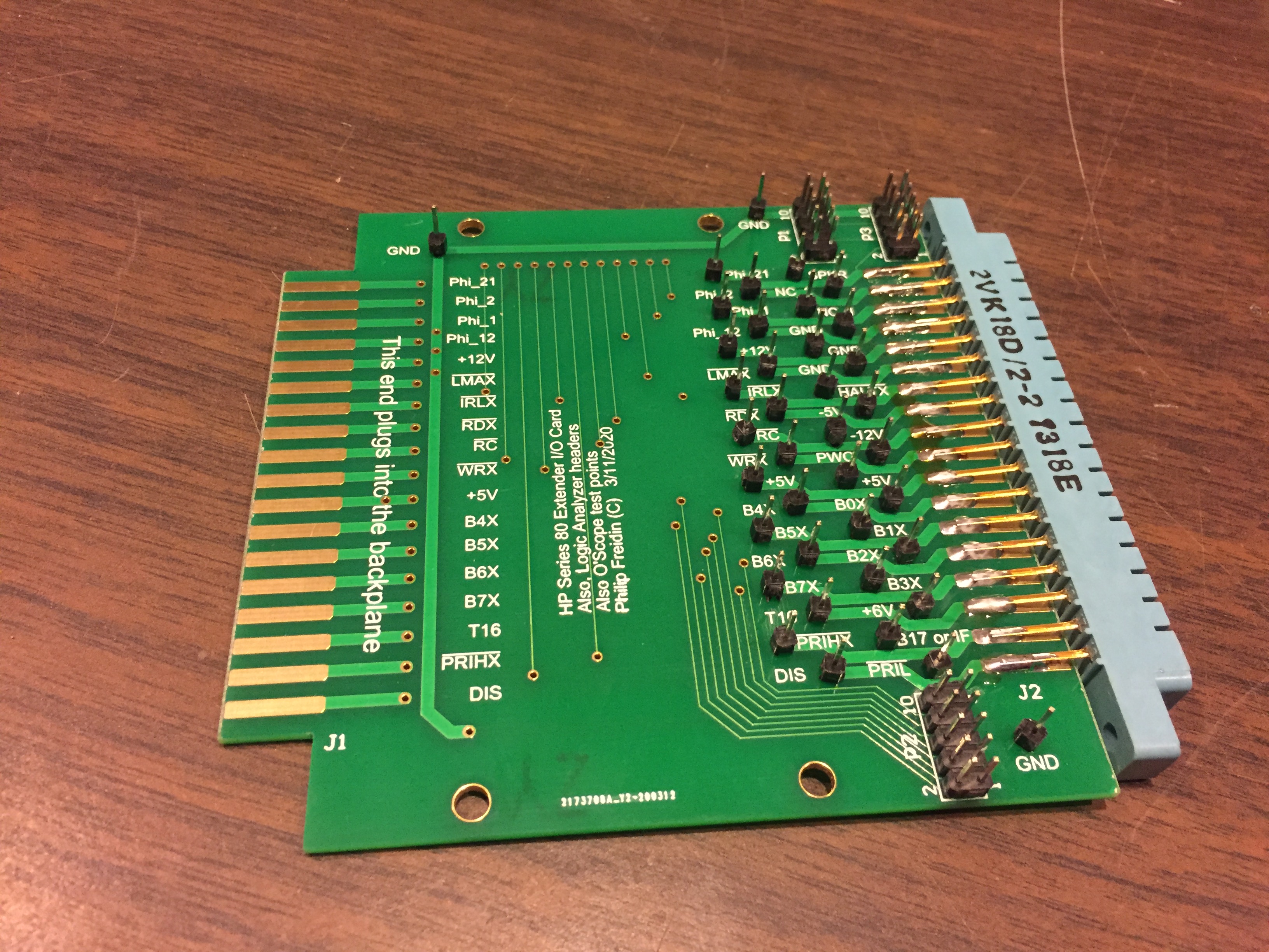
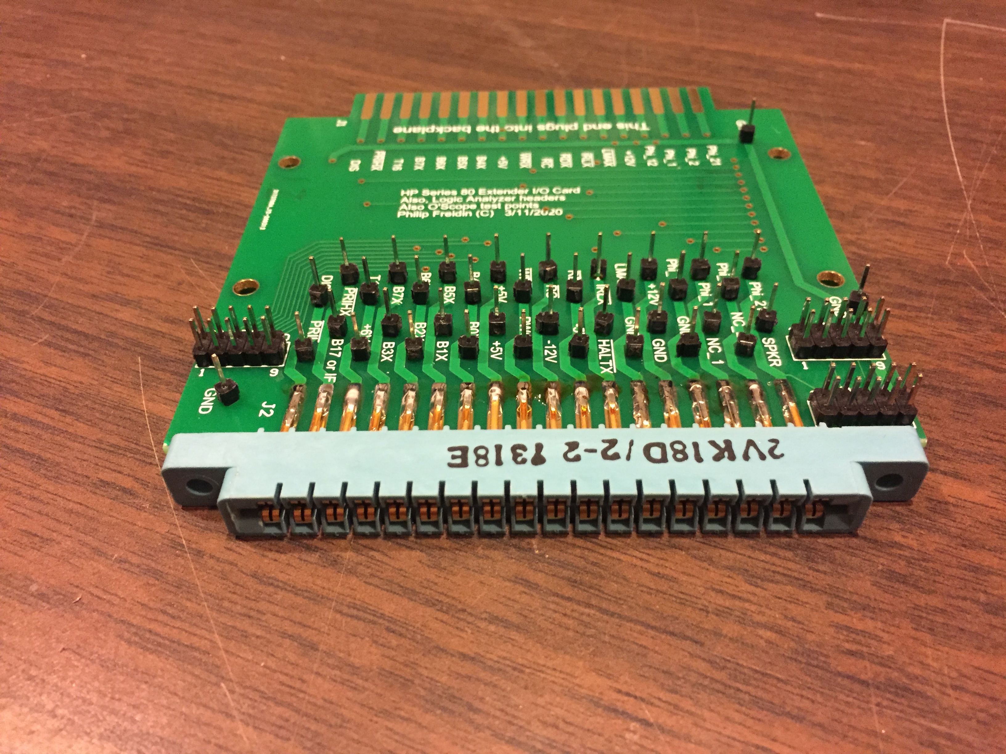
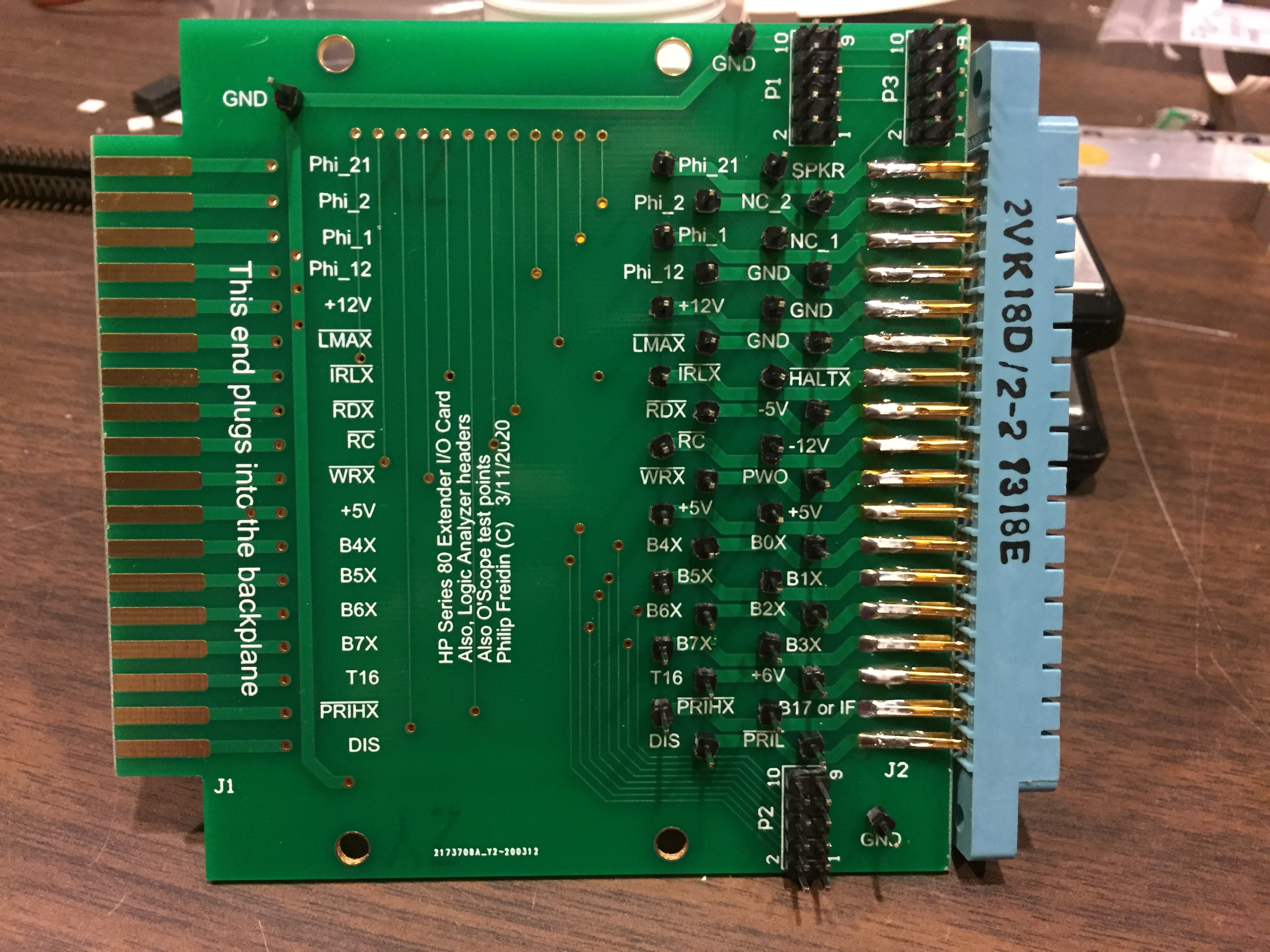
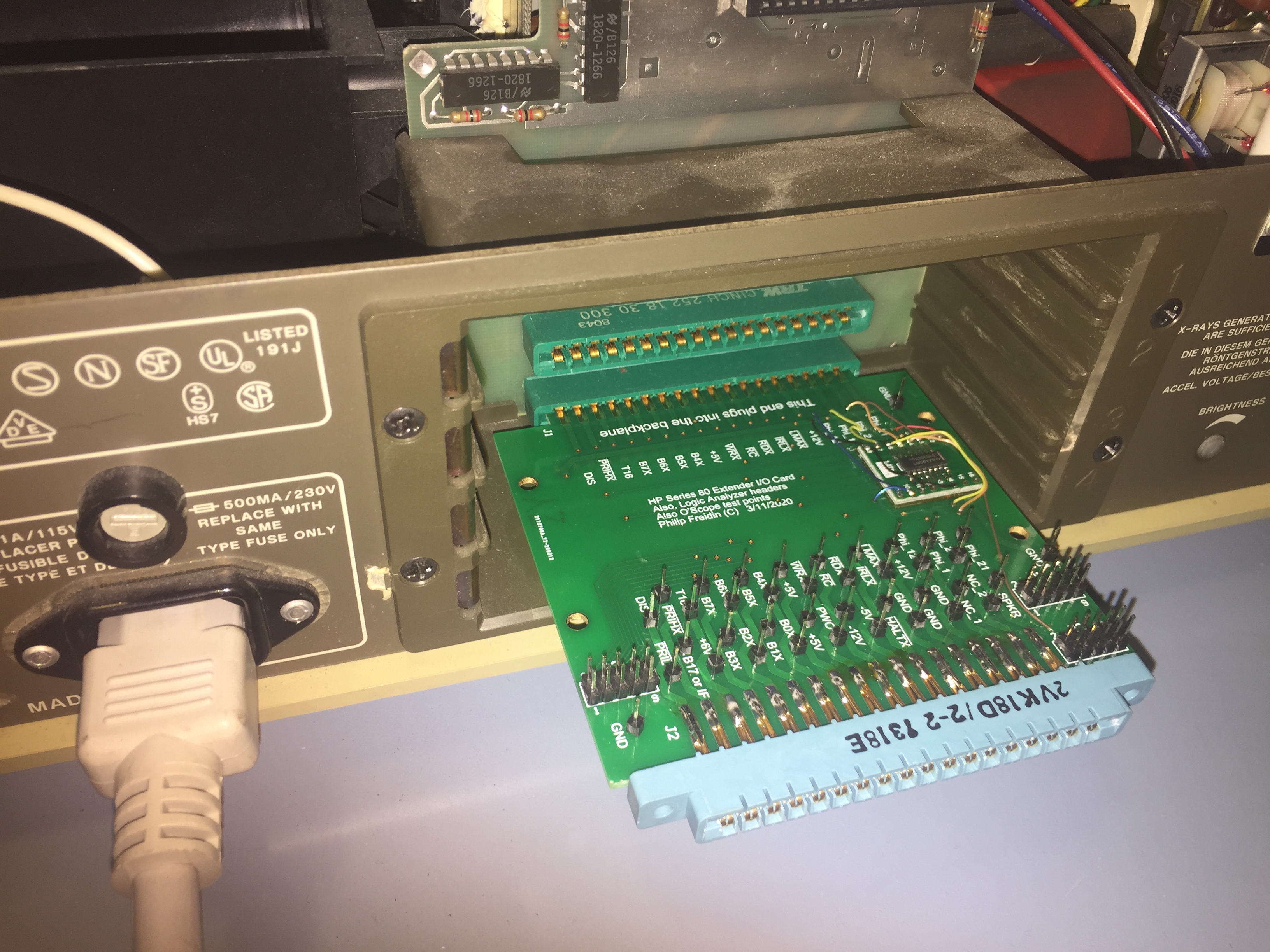
Currently this page is mostly a picture gallery for th HP85 I/O bus extender board I designed. The design is open source and all design files and manufacturing files can found in the GitHub Repository
The schematic can be downloaded with this link.
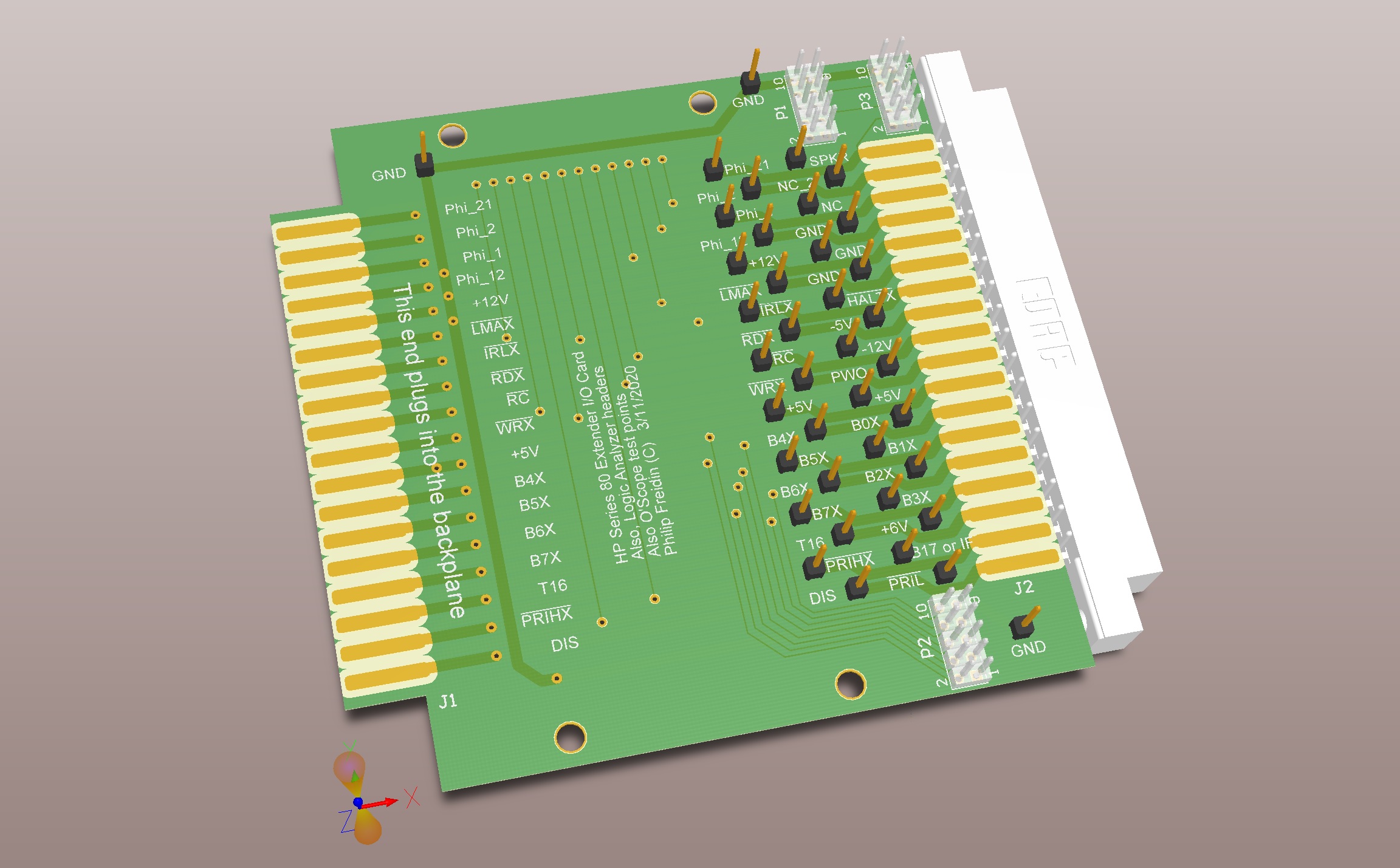
3D render of front of the Extender board
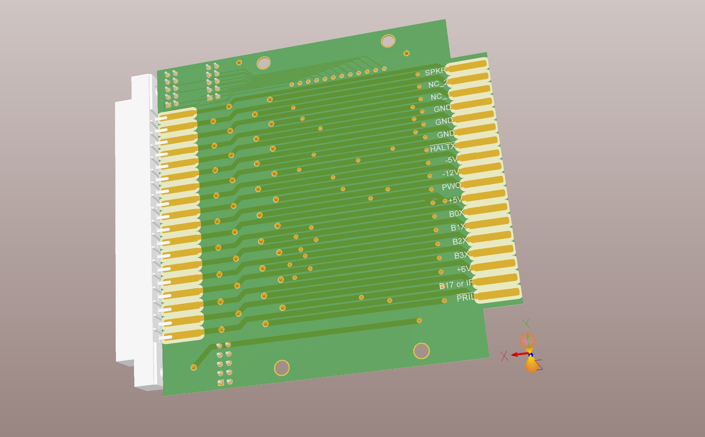
3D render of back of the Extender board
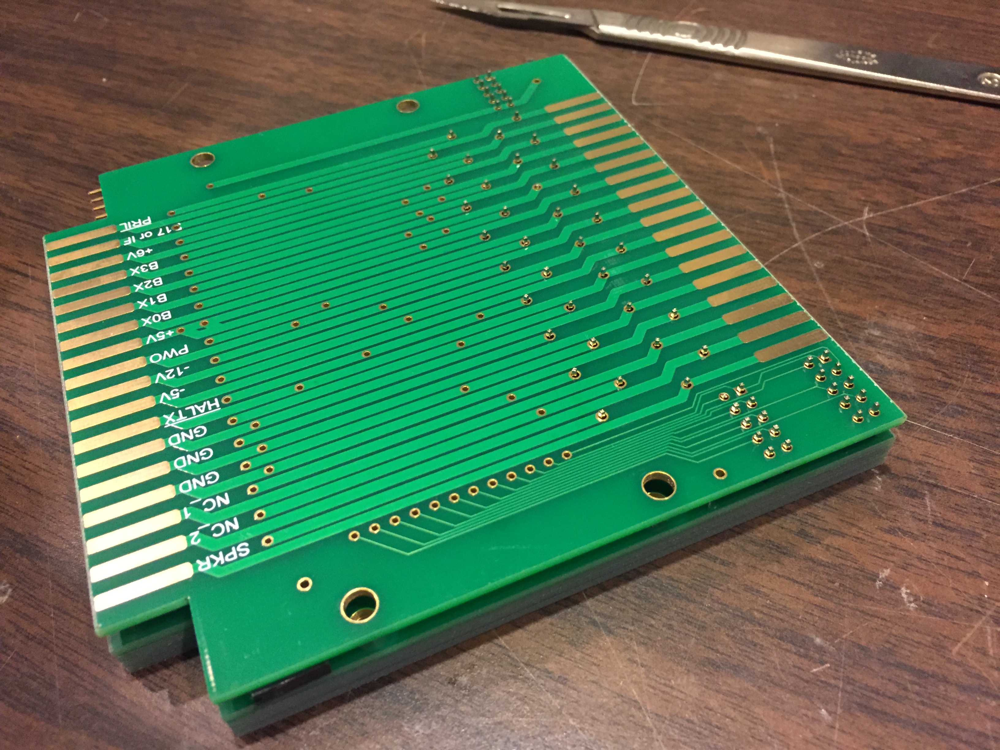
About to solder first board
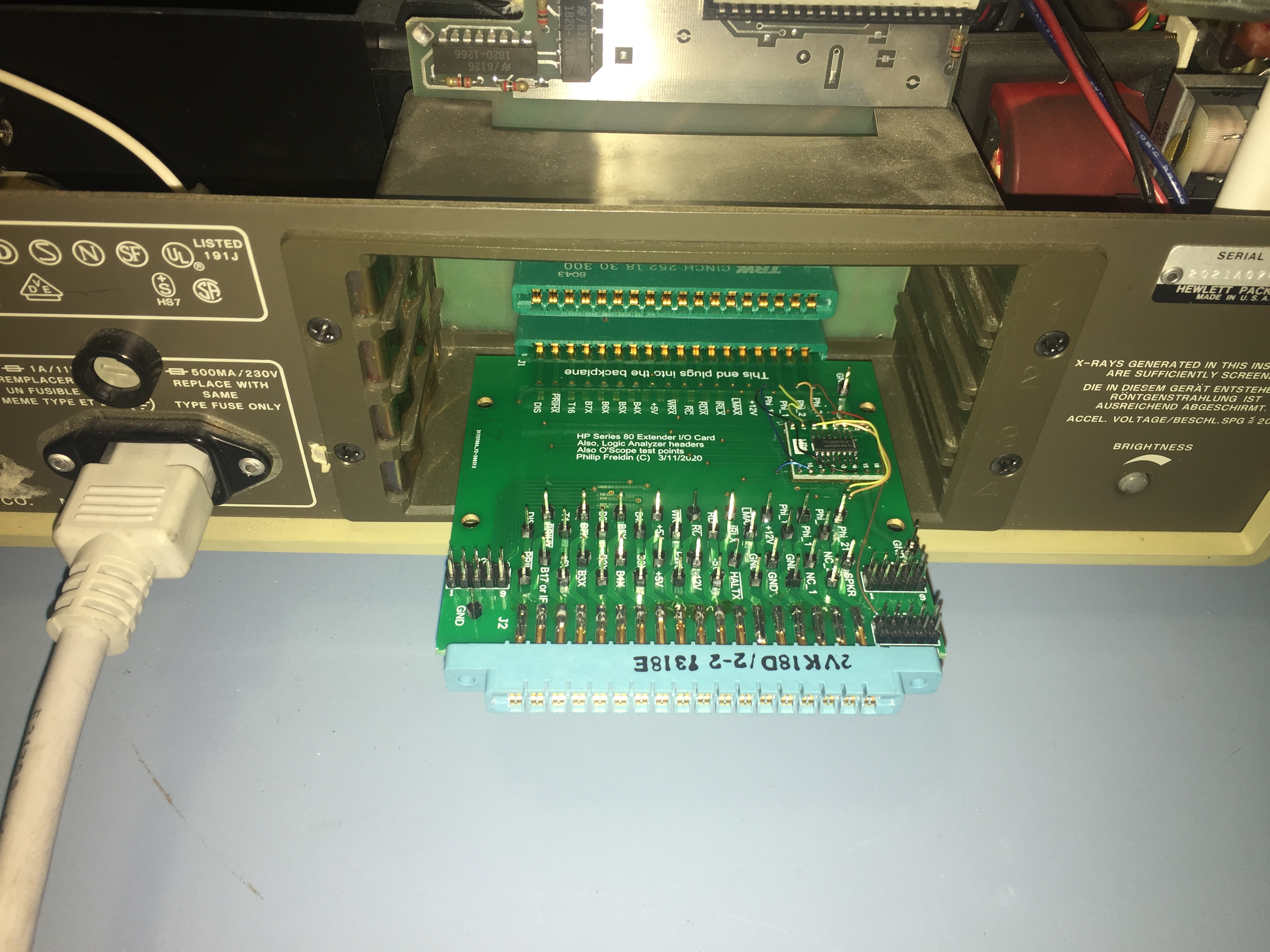
Clock lines level shifter
I forgot that the four clock lines are 12 volt signals that my el-cheapo logic analyzer would not to be able to handle. I added a CD4050BD in a SOIC package to do level shifting. The raw clock signals are still available on the individual pins and the level shifted versions (5 V max) are on the 2x10 headers for the logic analyzer.
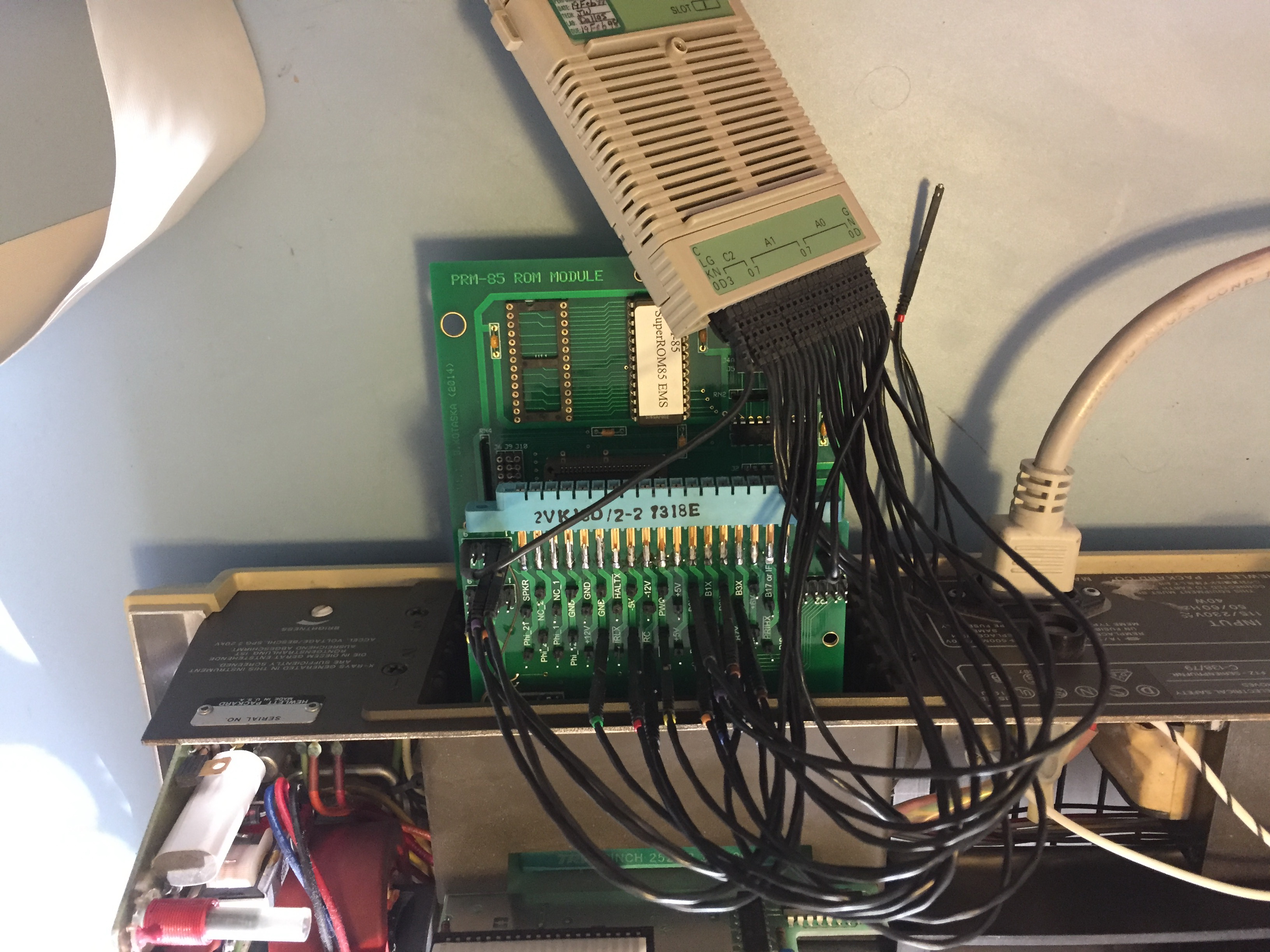
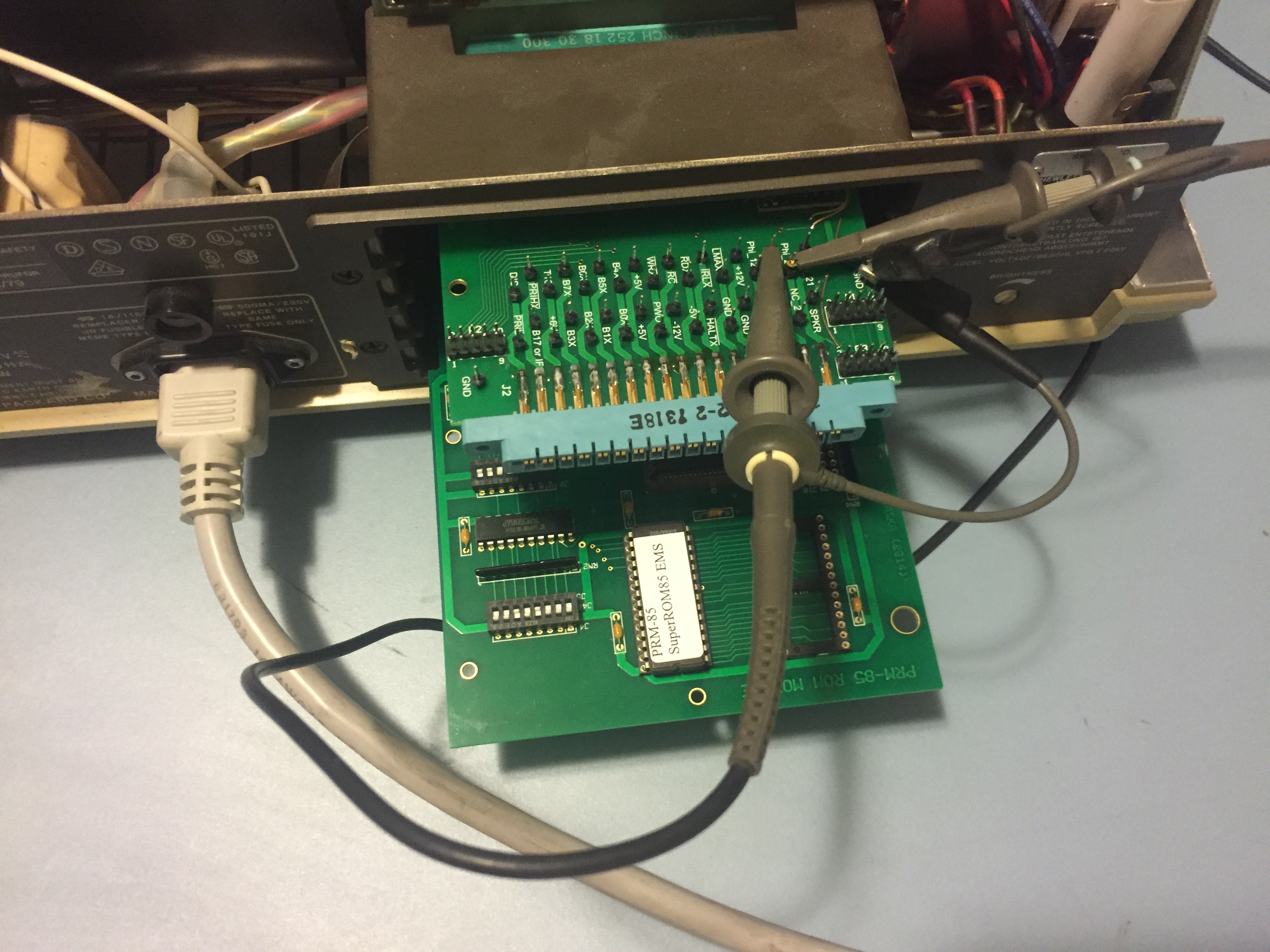
Example of use with 2 oscilloscope probes
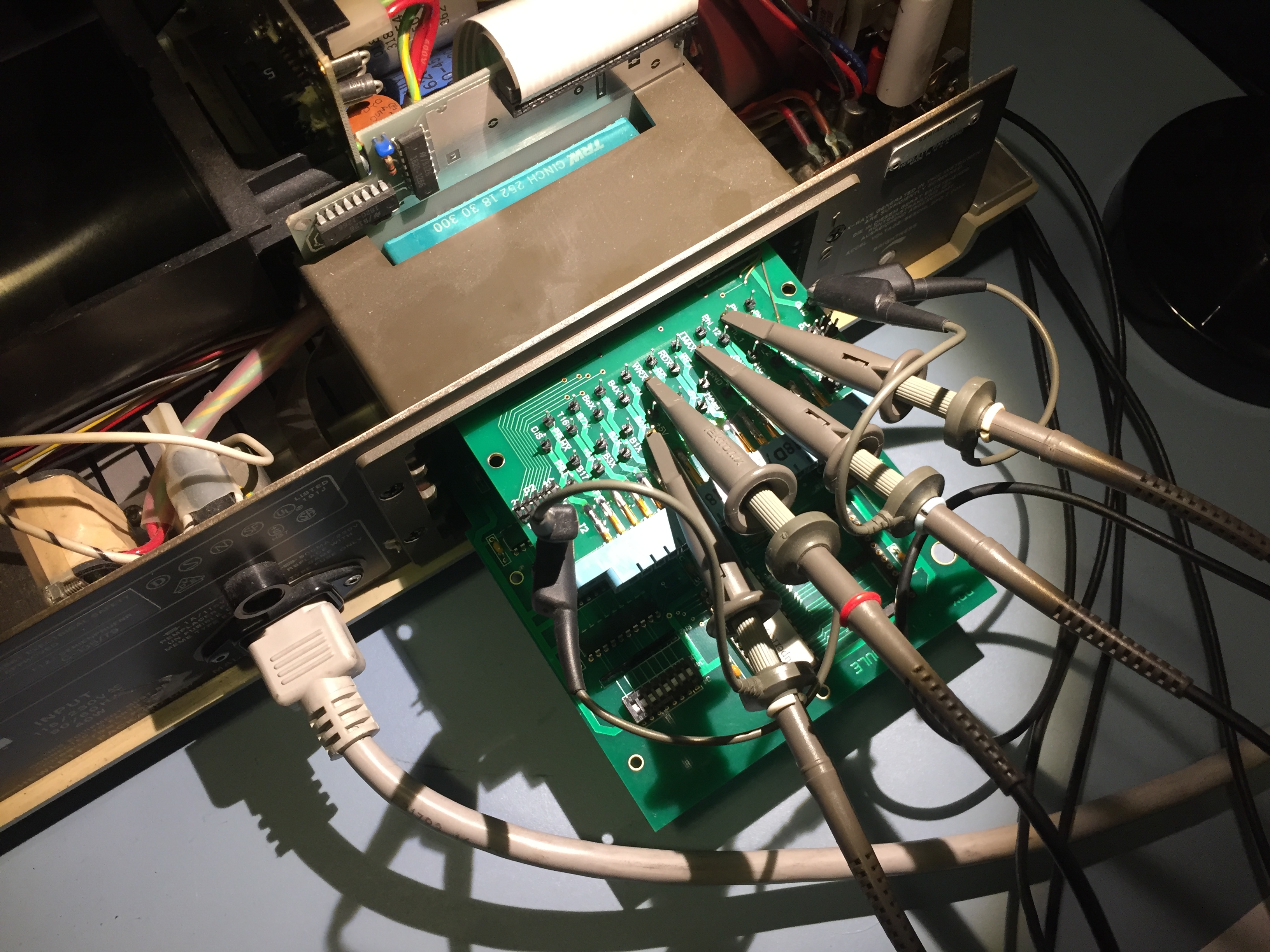
Example of use with 4 oscilloscope probes
Example of use with 4 oscilloscope probes and cheap Logic Analyzer
I have no explanation of how the 4 gray oscilloscope probes with the 3 apparently similar colored ID rings + red, show up as black probes with distinctive ID ring colors. Looking at them in normal room light, they look like above, gray with faded ID rings. Some sort of unknown magic must have happened when the next photo was taken. Really, no idea what happened. ??? I took some mor photos with various lighting that I have available with the same phone but I can’t replicate the coloring of the next picture. Must be space aliens.
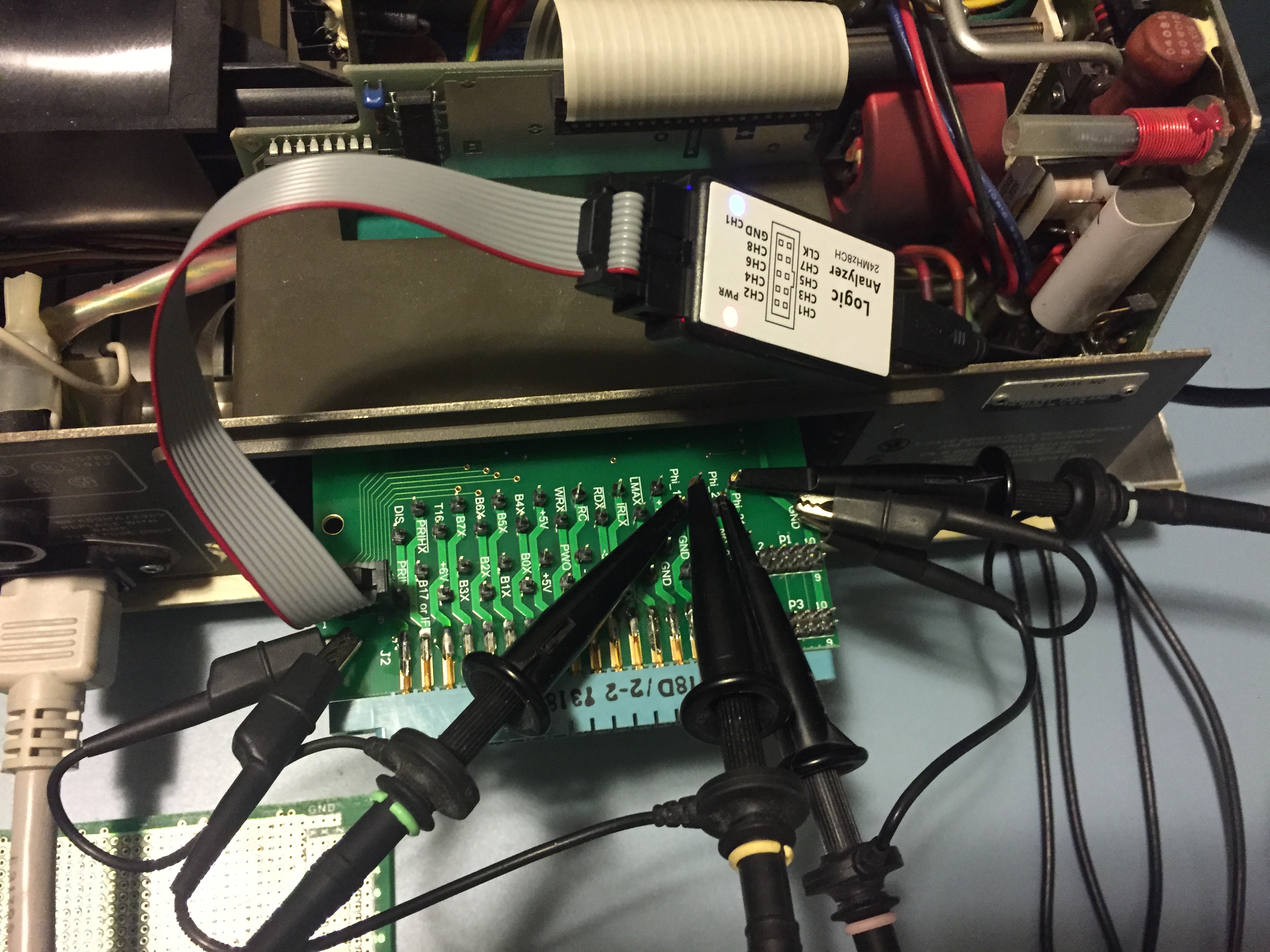
Example of use with fancy Logic Analyzer