Assembly
This page documents the process of assembling the Extender Board and doing the re-work to add a level shifter for the clock lines.
The four HP-85 clocks swing between 0 volts and 12 volts. The three 10-pin headers are intended to be used with a logic analyzer. If using a Cheap Logic Analyzer they are not designed to handle signals over 5 volts. The rework described on this page shows the changes to the extender board to add a CDCD4050 level shifter.
The schematic shows this in the bottom right corner.
If you only intend to use the extender pin with an oscilloscope or if you are using a logic analyzer that can handle 12 volt signals, you don’t need to make these modifications
Cut traces
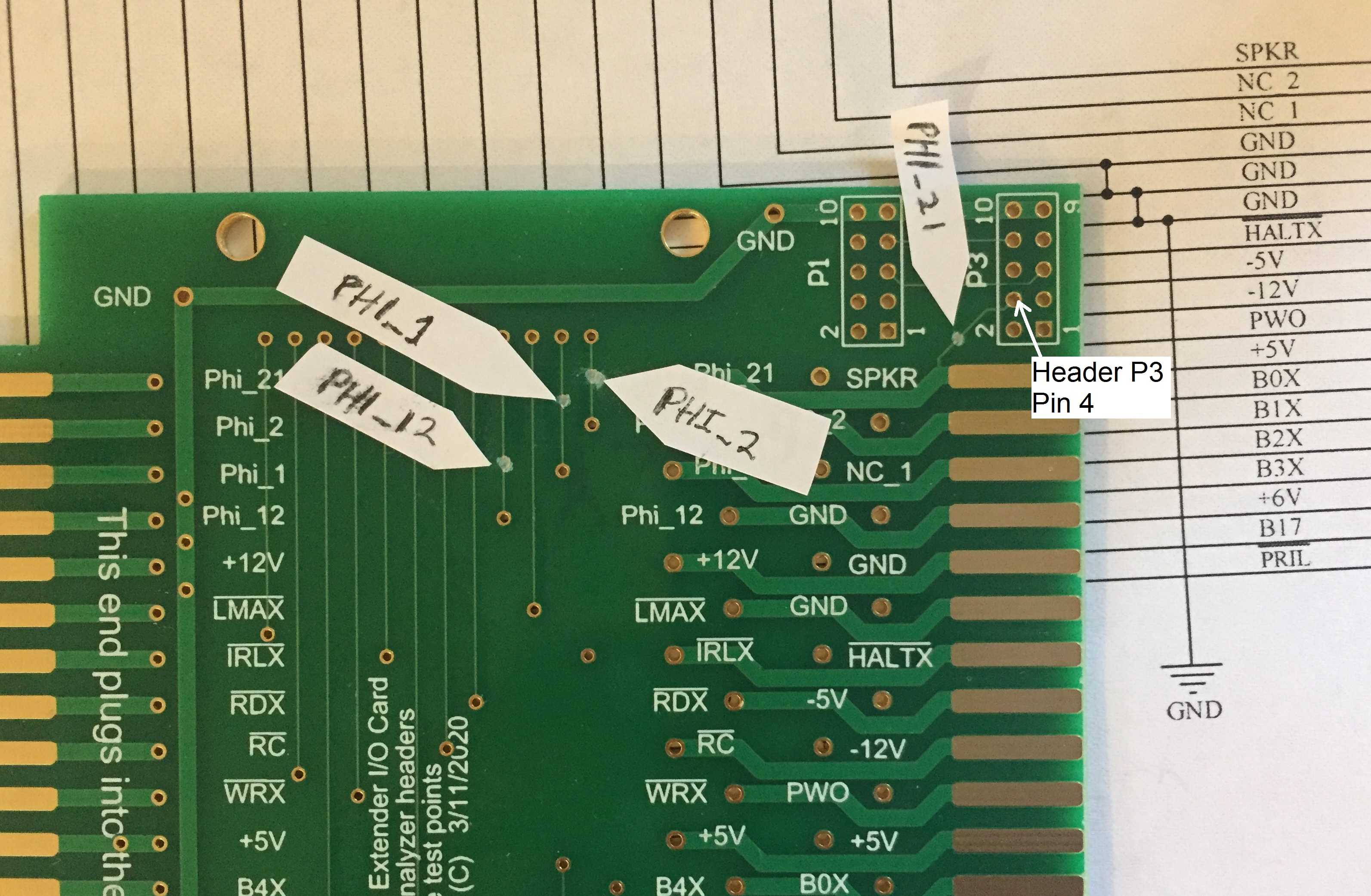
Cutting traces is only needed if you are going to be adding the CD4050 level shifter. The 4 traces need to be cut, one for each clock line, as marked in this photo. You can do this either with a sharp cutting tool, or as I have done in this example, with a Dremel with a very small round bur tip. Be careful to only cut in the 4 marked places
Install Pins and headers
There are 36 signal pins, 3 ground pins and 3 headers with 2x5 pins each. I have found a reasonable way to do the assembly is to first insert the 39 individual pins, and then press some corrugated cardboard down onto the pins untill they are all pushed into the cardboard. Then turn the assembly over and solder these 39 pins. Remove the cardboard, and insert and solder the 3 headers.
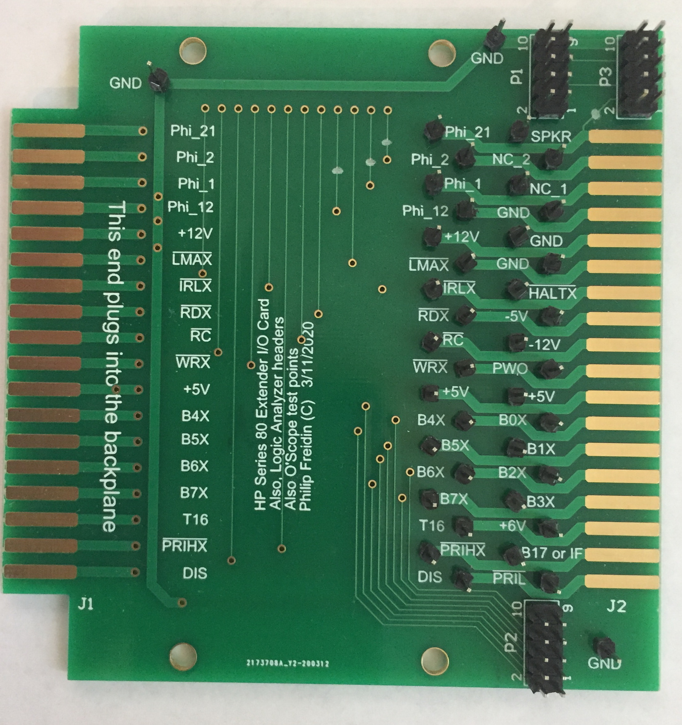
It is worth noting that all the pin labels are to the left or right of their respective pins. Not above or below
When using the extender and attaching logic analyzer or oscilloscope probes, always double check the label
Rework Details for the CD4050
This is the completed rework
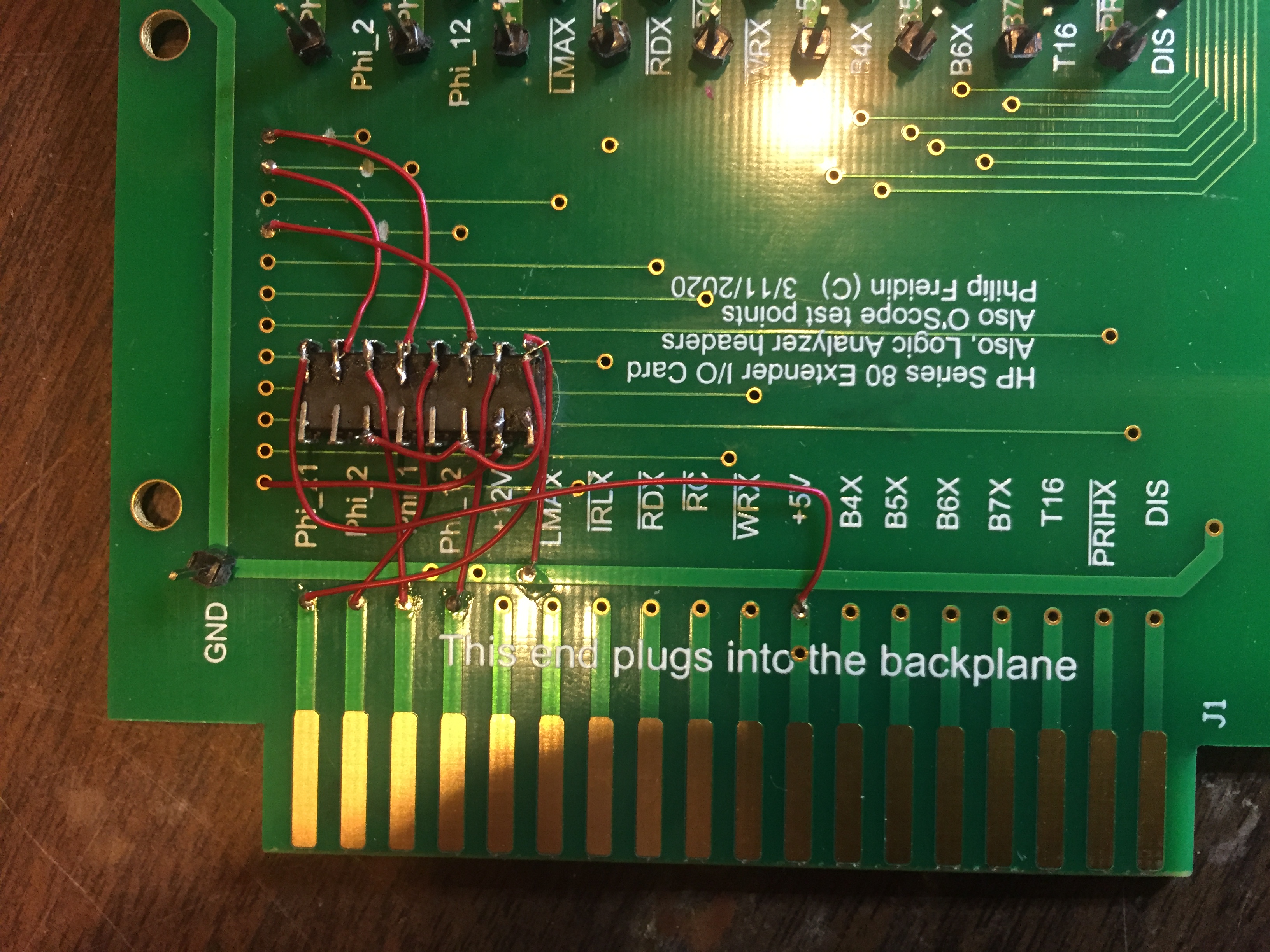
The first step is to place the CD4050 upside down and glue it to the PCB with super glue (cyanoacrylate) or maybe 2 part epoxy or hot melt glue. Remember that the pin numbers are flipped when you do this.
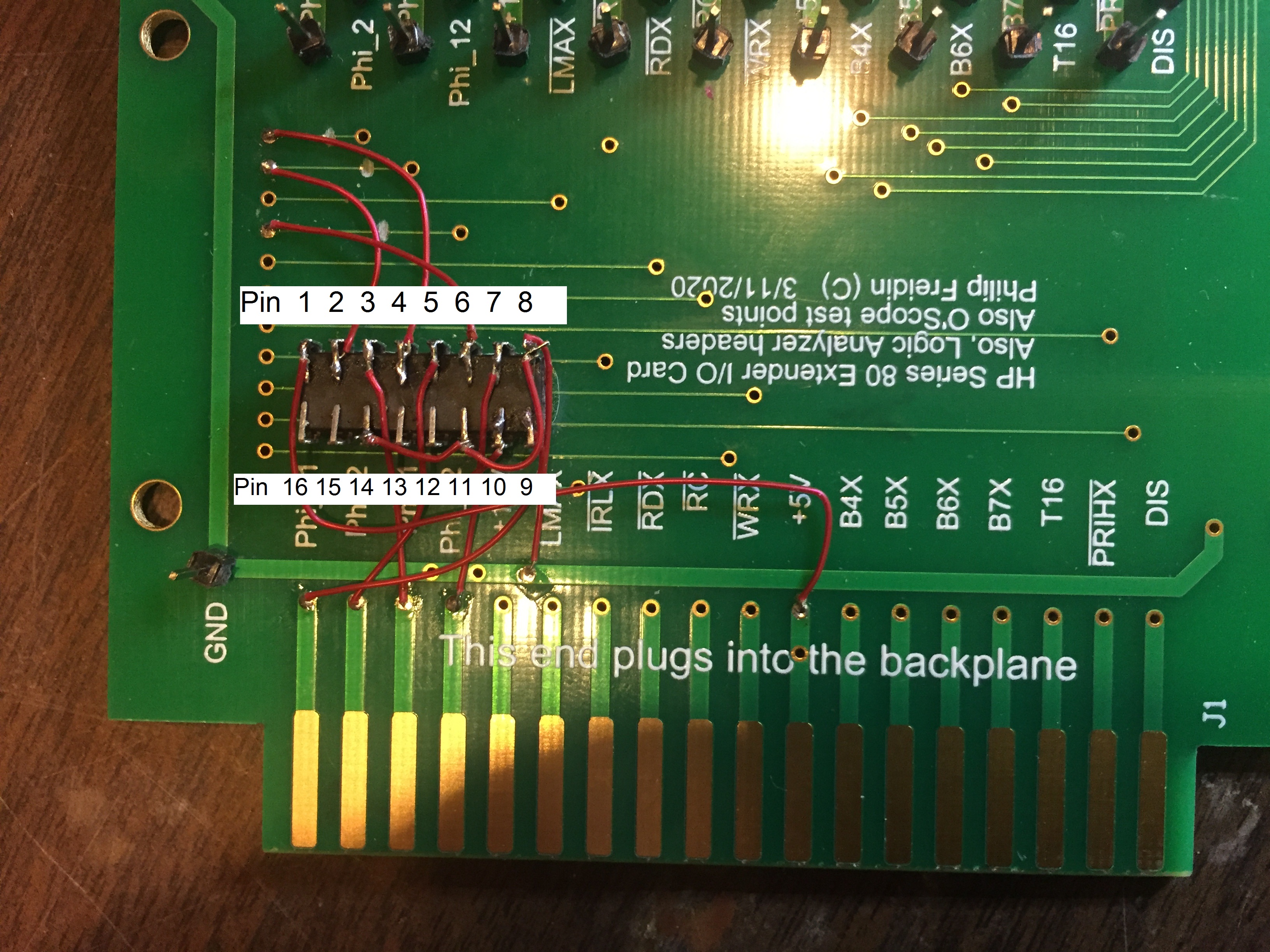
The 4 clock signals are picked up at the vias at the edge connector fingers and soldered to their respective pins (see schematic). I used Kynar insulation wire wrap wire, 30 AWG.
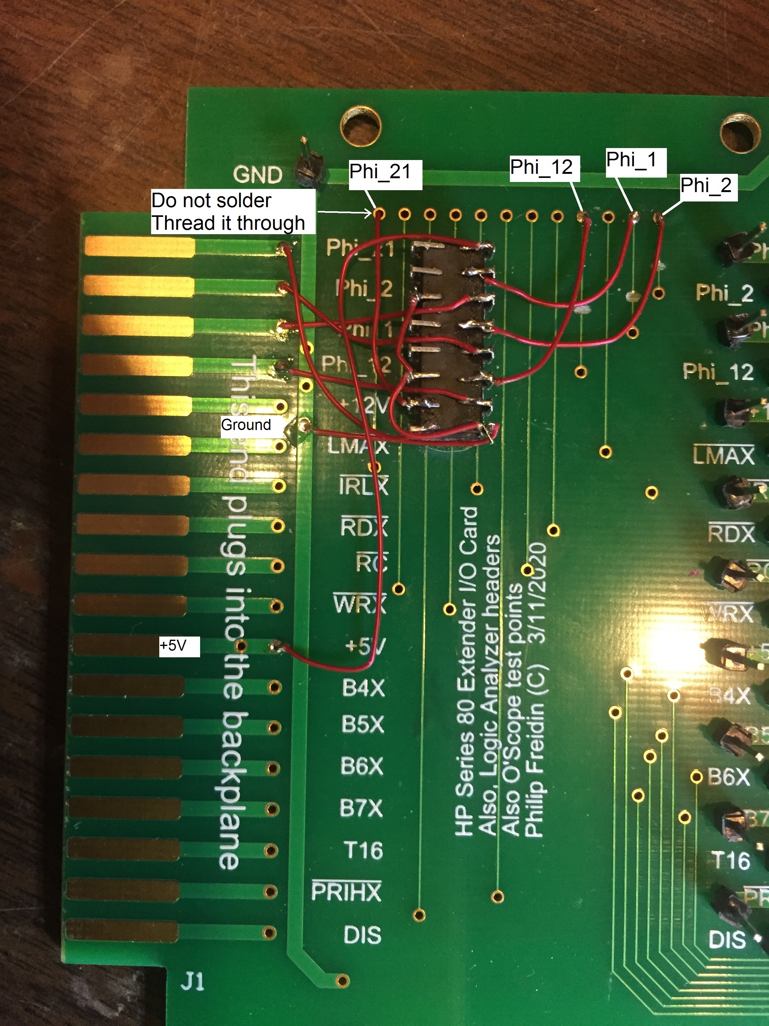
Three of the outputs of the level shifter are wired to the vias above where the thrace were cut. The fourth signal, level_shifted_Phi_21 has no convenient via on the top side of the board. Unlike the other three signals, it is threaded through the via shown and connected on the underside of the board to pin 4 of header P3. This pin is marked in the above photo
Connect Pin 1 of the CD4050 to the +5V signal (power into the CD4050) and a ground wire from pin 8, 11, and 14 to the ground trace. You can see a ground via next to the LMAX label.
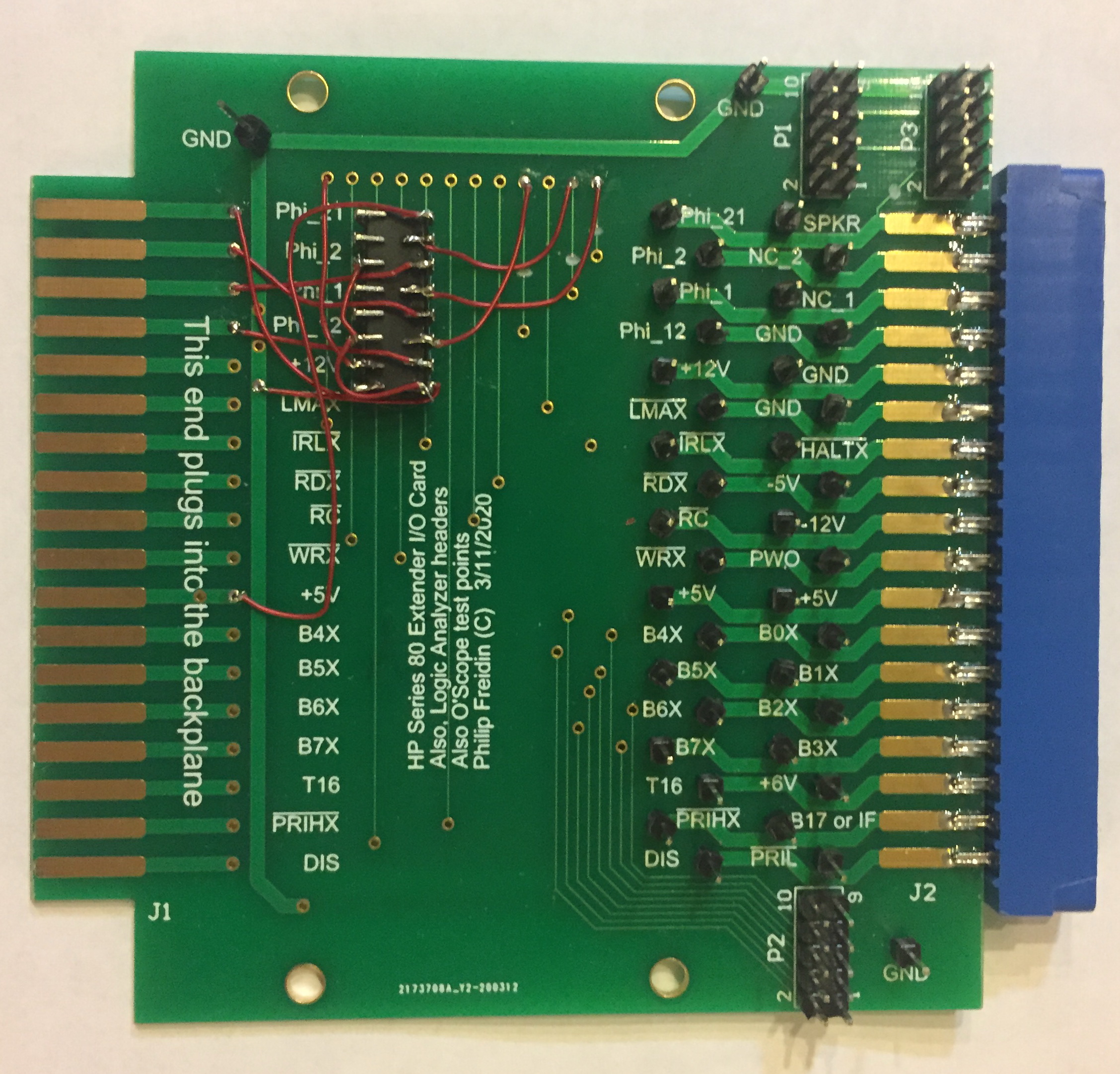
When adding the 36 pin connector, you may need to bend the two rows of pins toward each other to match the thickness of the board. This is best done before you start soldering this connector.