HP85 I/O Bus Timing
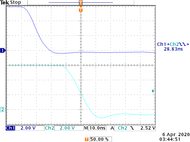
Delays through 1MA8
| Timing Paths through 1MA8 | Name | Typical |
|---|---|---|
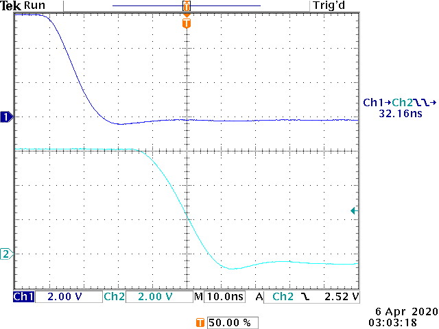
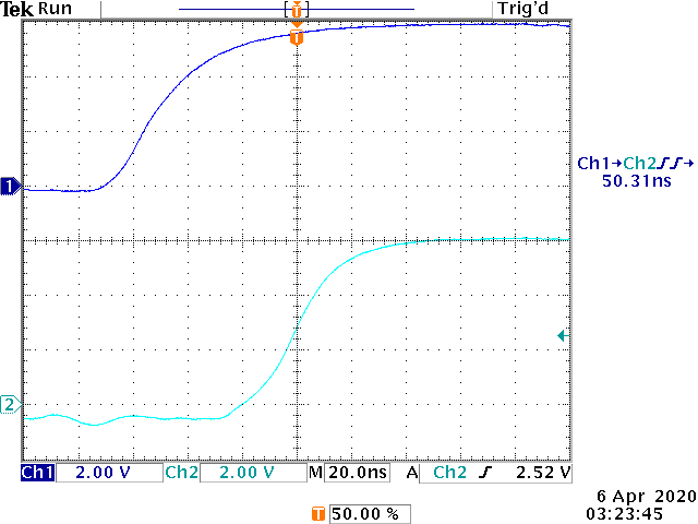
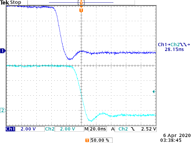
| /LMA Falling Edge | TLMAF | 32 ns |
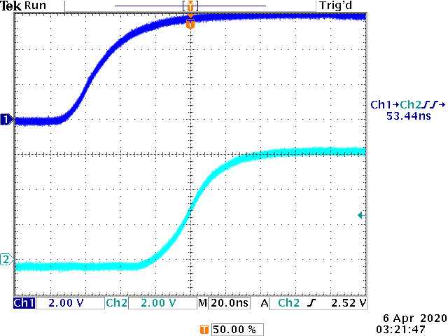
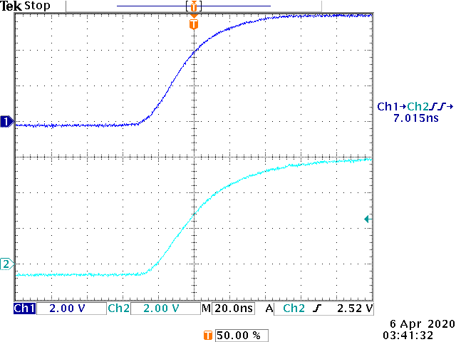
| /LMA Rising Edge | TLMAR | 53 ns |
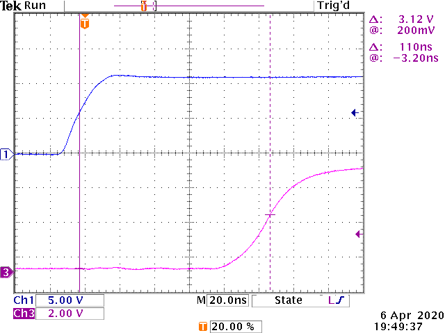
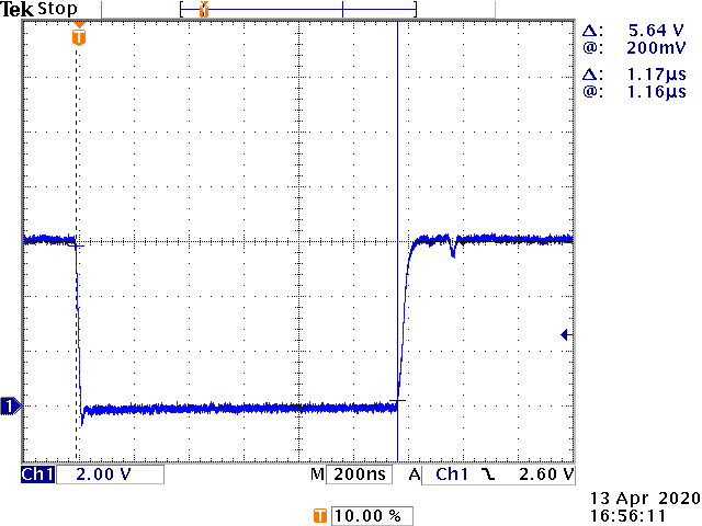
| LMA Pulse Width on I/O bus |
TLMAPW | 1.17 us |
Source Oscilloscope images
| Timing Paths through 1MA8 | Name | Typical |
|---|---|---|
| RD Falling Edge | TRDF | 28 ns |
| RD Rising Edge | TRDR | 50 ns |
| RD Pulse Width | TRDPW | 1.19 us |
Source Oscilloscope images
| Timing Paths through 1MA8 | Name | Typical |
|---|---|---|
| WR Falling Edge | TWRF | 29 ns |
| WR Rising Edge | TWRR | 49 ns |
| WR Pulse Width | TWRPW | 1.17 us |
Source Oscilloscope images
| Timing Paths through 1MA8 | Name | Typical |
|---|---|---|
| B0 Falling Edge | TDATAF | 28 ns |
| B0 Rising Edge | TDATAR | 7 ns |
Source Oscilloscope images
Write Cycle as seen on the I/O bus
These timing measurements are from the CPU writing to RAM or I/O as seen on the I/O bus. These signals have all passed through the 1MA8 except for the 4 clock signals. TON is therefor under control of the 1MA8. The data being written from the CPU actually stops being actively driven on the falling edge of Phi 1. The data remains valid for the next 200 ns because the bus has no drivers for that 200 ns (Bus Float states have no bus drivers, and there are no passive loads like pull-down or pull-up resistors)
Note:
     FP    Float Prior, Extend prior data value but without active drive
     FD    Float Data, Extend prior data value but without active drive
     PC    Pre-Charge (drive to 6V)
     FH    Float High, Extend prior Pre-Charge
| Write cycle data setup and hold | Name | Typical |
|---|---|---|
| Data Setup | TON | 80 ns |
| Data Setup | TSU | 120 ns |
| Data Hold | THOLD | 200 ns |
Source Oscilloscope images
Address Cycle as seen on the I/O bus
These timing measurements are from the CPU sending Address bytes as seen on the I/O bus. These signals have all passed through the 1MA8 except for the 4 clock signals. TON is therefor under control of the 1MA8. The addresses being written from the CPU actually stops being actively driven on the falling edge of Phi 1. The address remains valid for the next 200 ns because the bus has no drivers for that 200 ns (Bus Float states have no bus drivers, and there are no passive loads like pull- down or pull-up resistors)
Note:
     FP    Float Prior, Extend prior data value but without active drive
     FD    Float Data, Extend prior data value but without active drive
     PC    Pre-Charge (drive to 6V)
     FH    Float High, Extend prior Pre-Charge
| Write cycle data setup and hold | Name | Typical |
|---|---|---|
| Data Setup | TON | XX ns |
| Data Setup | TSU | XXX ns |
| Data Hold | THOLD | 200 ns |
Source Oscilloscope images
Need to come back and re-do the oscilloscope pictures for thisOther Timing Measurements
Source Oscilloscope images
Detailed instruction Fetch and Execute
HP85 Instruction Fetch and Execute Overview
In the Advanced Programming ROM at effective address 0x7E87
is the following byte sequence
  Hex:     5E  B0  99  82
  Octal:  136 260 231 202

The instruction is            LDBD R36,=0x8299    (a RAM location)

The bus cycle of 1600 ns
Values given in Hex except for the destination register which is 36 octal
The data values appear on the bus during the Phi 1 period following
the /LMA or /RD
Issue /LMA, Data is 87          Low 8 bits of the address of the instruction
Issue /LMA, Data is 7E          High 8 bits of the address of the instruction
Issue /RD,  Data is 5E          First of 4 bytes of the insruction. This is
                                DRP 36 which is specifying the destination register
Bus is idle for 1 cycle
Issue /RD,  Data is B0          Second of 4 bytes of the insruction. This is
                                LDBD with an immediate memory address to follow
Issue /LMA & /RD, Data is 99    Third of 4 bytes of the insruction. This is the
                                low 8 bits of the address in RAM that will be fetched
                                Note that the /RD is reading the byte from ROM, and
                                simultaneously the /LMA is telling all devices on
                                the bus that a new 16 bit address is being issued
Issue /LMA & /RD, Data is 82    Fourth of 4 bytes of the insruction. This is the
                                high 8 bits of the address in RAM that will be fetched
                                The RAM controller will match this address
Issue /RD,  Data is 04          Read the RAM at address 0x8299, returned value is 04
The LDBD R36,=Address instruction reads a byte from the specified address and places it into register 36. The instruction is 4 bytes long
The instruction bytes are stored at Hex 7E87 through to 7E8A
Byte 1: Specifies R36 (0x5E)
Byte 2: Specifies the instruction LDBD, with addressing mode Literal Direct (0xB0)
Byte 3: Specifies the low 8 bits of the direct address (0x99)
Byte 4: Specifies the high 8 bits of the direct address (0x82)
Scroll the following timing diagram to see the complete sequence of events.
Oscilloscope screen captures
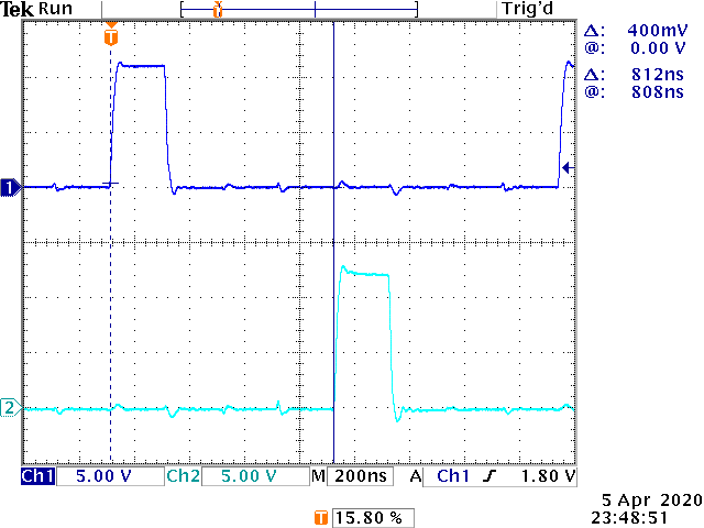
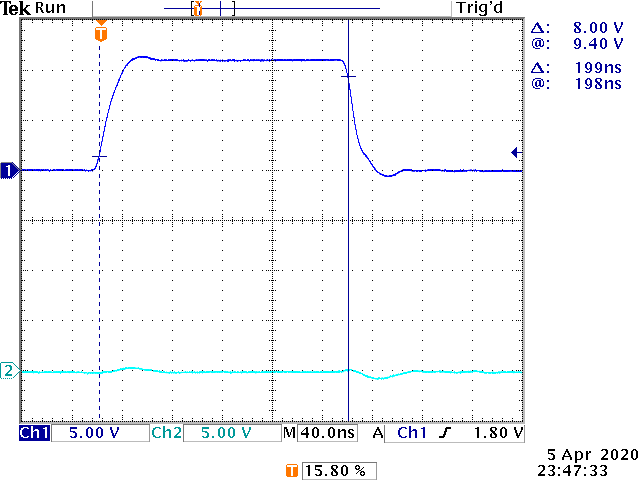
LMA Falling Delay
Channel 1: /LMA on mainboard
Channel 2: /LMAX on I/O bus
LMA Rising Delay
Channel 1: /LMA on mainboard
Channel 2: /LMAX on I/O bus
LMA Pulse Width
Channel 1: /LMAX on I/O bus
RD Falling Delay
Channel 1: /RD on mainboard
Channel 2: /RDX on I/O bus
RD Rising Delay
Channel 1: /RD on mainboard
Channel 2: /RDX on I/O bus
RD Pulse Width
Channel 1: /RDX on I/O bus

WR Falling Delay
Channel 1: /WR on mainboard
Channel 2: /WRX on I/O bus
WR Rising Delay
Channel 1: /WR on mainboad
Channel 2: /WRX on I/O bus

WR Pulse Width
Channel 1: /WRX on I/O bus
Data Falling Delay
Channel 1: B0 on mainboard
Channel 2: B0X on I/O bus
Data Rising Delay
This does not seem right. Need to re-measure this parameter.
Channel 1: B0 on mainboad
Channel 2: B0X on I/O bus
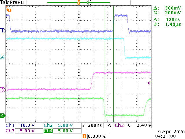
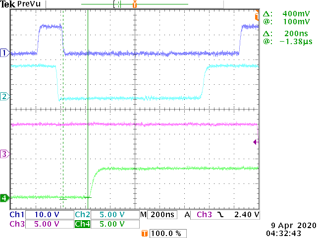
Data Setup
Channel 4 shows the latest falling edge for data on the I/O bus. While some devices provide data earlier, from the point of view of someone desiging an I/O device, the latest arrival time is what is important. The Capricorn processor is responsible for these latest valid data. Also, note that an example of data from Capricorn are the address bytes. I/O devices, RAM and ROM, all provide data sooner (but from a design point of view, you must work with the latest valid data situation). Capricorn provides valid data about 150 ns prior to the rising edge of Phi 1. After passing through the I/O bus controller chip (1MA8, IC U1), data is seen going valid on the I/O bus 120 ns before the rising edge of Phi 1.
Channel 1: Phi 1
Channel 2: /LMAX
Channel 3: /WRX
Channel 4: Data on I/O bus
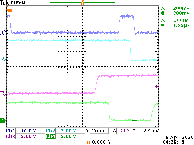
Data Hold
Channel 4 shows Data Hold time after the falling edge of Phi 1, on the I/O bus. The timing is the same on the data pins of Capricorn. This is because the bus drivers on both the I/O bus, and Capricorn have already turned off about 50 ns to 150 ns after the falling edge of Phi 1, and the both busses (I/O and main board) are undriven, and are just holding their value due to bus capacitance and a lack of resistive load. On the rising edge of Phi 12 (200 ns after the falling edge on Phi 1) the pre-charge drivers are enabled on both busses, and all data lines on both busses are pre-charged high. Any device on either bus can reliably capture data with the falling edge of Phi 1.
Channel 1: Phi 1
Channel 2: /LMAX
Channel 3: /WRX
Channel 4: Data on I/O bus
Address Setup
Need to make this measurementAddress Hold
Channel 1: Phi 1
Channel 2: /LMAX
Channel 3: /WRX
Channel 4: Data on I/O bus
Phi 1 and Phi 2 relative timing
Channel 1: Phi 1
Channel 2: Phi 2
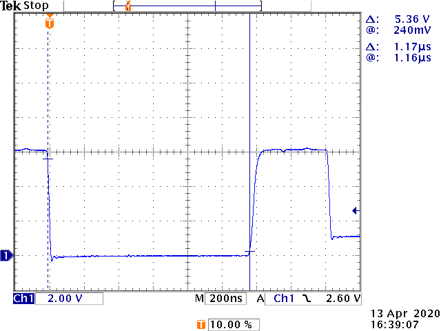
Phi 1 is a 200ns Pulse
Channel 1: Phi 1
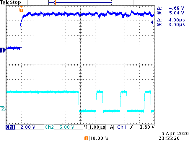
Delay from PWO high to First /LMA is 4us
Channel 1: PWO
Channel 2: /LMA
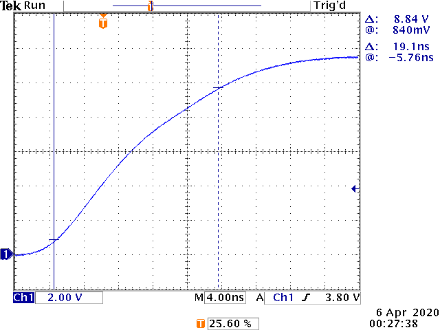
Phi 1 Rise time is 19ns
Channel 1: Phi 1
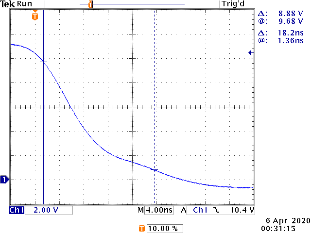
Phi 1 Fall time is 18ns
Channel 1: Phi 1
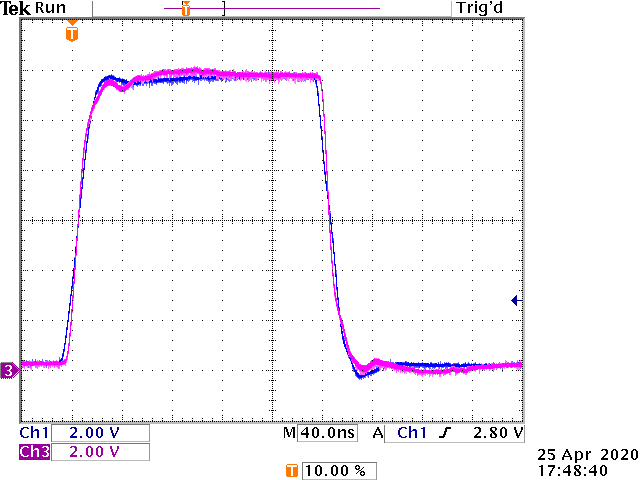
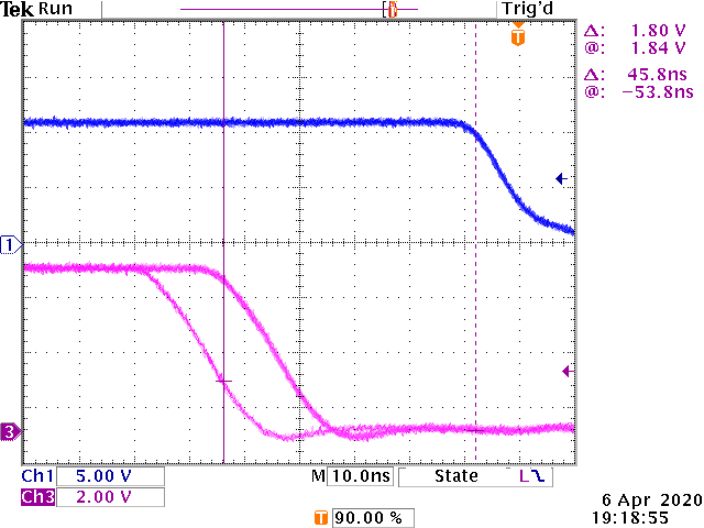
Phi 1 on Mainboard and on I/O Bus
Channel 1: Phi 1 on mainboard (Blue)
Channel 3: Phi 1 on I/O bus extender (Pink)
LMAX Falling edge Spread (or Jitter) 12 ns
Channel 1: Phi 1
Channel 3: /LMAX (/LMA on I/O Bus)

LMAX Earliest Falling edge to Phi 1 Falling edge 43 ns
Channel 1: Phi 1
Channel 3: /LMAX (/LMA on I/O Bus)
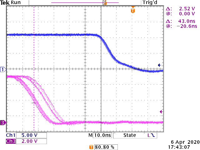
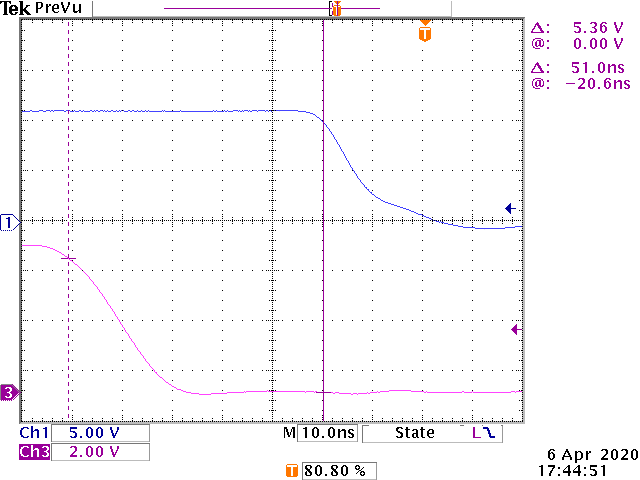
LMAX Average Falling edge to Phi 1 Falling edge 51 ns
Channel 1: Phi 1
Channel 3: /LMAX (/LMA on I/O Bus)
WRX Falling edge Spread (or Jitter) (none)
Channel 1: Phi 1
Channel 3: /WRX (/WR on I/O Bus)
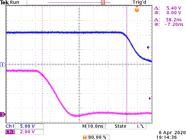
WRX Falling edge to Phi 1 Falling edge 58 ns
Channel 1: Phi 1
Channel 3: /WRX (/WR on I/O Bus)
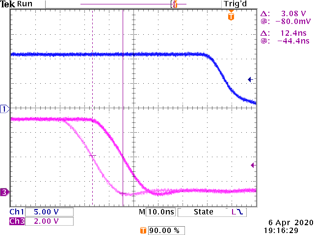
RDX Falling edge Spread (or Jitter) 12 ns
Channel 1: Phi 1
Channel 3: /RDX (/RD on I/O Bus)
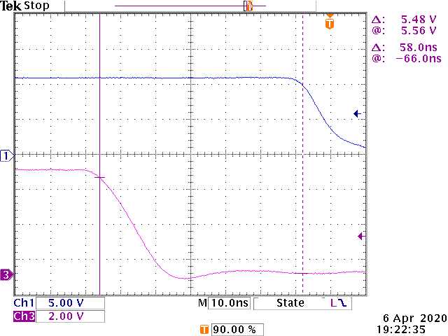
RDX Earliest Falling edge to Phi 1 Falling edge 46 ns
Channel 1: Phi 1
Channel 3: /RDX (/RD on I/O Bus)
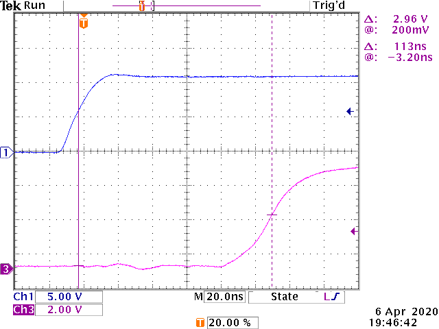
LMAX Rising edge after Phi 21 Rising edge 113 ns
Channel 1: Phi 21
Channel 3: /LMAX (/LMA on I/O Bus)

RDX Rising edge after Phi 21 Rising edge 113 ns
Channel 1: Phi 21
Channel 3: /RDX (/RD on I/O Bus)
WRX Rising edge after Phi 21 Rising edge 110 ns
Channel 1: Phi 21
Channel 3: /WRX (/WR on I/O Bus)